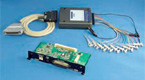
OP-SB85 TTL/I2C/SPI Expansion Kit
[ Discontinued ]
The successor is OP-SB85L.
The successor is OP-SB85L.
Outline
The kit incorporates a high-speed analog signal measurement function operating at a maximum of 40M samples per second, which is ideal for the analog waveform analysis of communications signals.
Operating Instructions
Monitor function
| Normal mode (USART) allows to use all functions such as trigger function. BURST mode allows to measure clock SYNC which is not supported in former models. (Clock SYNC: clock is given only when transmitting data.) I2C mode allows to measure I2C serial communications with start/ stop sequence. I2C and SPI communication can be displayed in translation display and it is possible to analysis read and write sequence. | 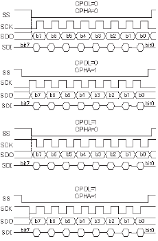 The timing of clock and data set at “CPOL” and “CPHA” is described in above figure. |
||||||||||||||||||
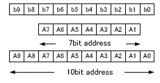 The relation of input data and address is as follows. e.g.) Input “123”; [If 7 bit] “0010001” is set. [If 10 bit] “0100100011” is set. |
|||||||||||||||||||
[ I2C Monitor ]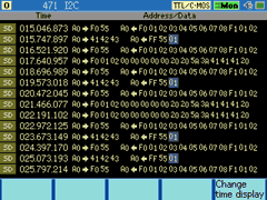 |
[ SPI Monitor ]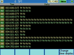 |
||||||||||||||||||
|
|
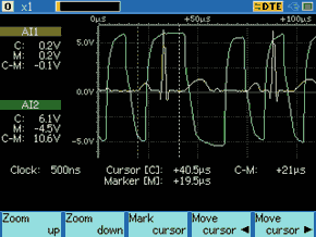
Analog Waveform Analysis
Simulation / Bert
Excepting the BURST mode, using the simulation function enables you to vastly enhance the efficiency of the development and the trouble analysis. In the I2C and SPI mode, you can simulate in both the master and the slave. Also, since the bit error rate test (BERT) is available in the normal mode (USART), you can easily test the transmission feature of the device, etc.Specification
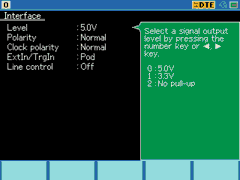
| Interface | TTL, I2C, SPI (connected with test clips) |
|---|---|
| Input impedance | 100K Ohm |
| Input Level Threshold | High: 2.2 V min. Low: 0.9 V max. (Maximum input: (-1V ~ +7V) |
| Output Level Voltage | High: 3.0 V, 4.5 V, without pull-up Low: 0.5 V max. |
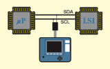
| Probe Signal | SD (SDA/SDO), RD (SDI), RTS (SS), CTS, EXIN, TXC (SCL/SCK), RXC, TRG.IN,TRG.OUT(Lead length: 170 mm) |
| Expansion protocol | I2C, SPI, Burst (*1) |
| Communications test function | Monitor/Simulation/BERT (*2) |
| Speed (I2C Test) | 100Kbps, 400Kbps, 1Mbps |
| Speed (SPI test) | 10 Mbps max. |
| Analog waveform analysis | The signal voltages of 2 channels are measured and displayed in analog waveform Sampling: 1 MHz to 40MHz (in 6 steps), 4K points Measurement range: ±6 V/±12 V |
| Composition | Dedicated expansion board, relay cable, high-speed TTL probe pod, 3-wire probe cable |
*2: No I2C, SPI, or Burst BERT testing supported.